- 您现在的位置:买卖IC网 > Sheet目录3889 > PIC18C452T-E/L (Microchip Technology)IC MCU OTP 16KX16 A/D 44PLCC
2001 Microchip Technology Inc.
DS39026C-page 107
PIC18CXX2
13.0
CAPTURE/COMPARE/PWM
(CCP) MODULES
Each CCP (Capture/Compare/PWM) module contains
a 16-bit register which can operate as a 16-bit capture
register, as a 16-bit compare register, or as a PWM
master/slave Duty Cycle register. Table 13-1 shows the
timer resources of the CCP module modes.
The operation of CCP1 is identical to that of CCP2, with
the exception of the special event trigger. Therefore,
operation of a CCP module in the following sections is
described with respect to CCP1.
Table 13-2 shows the interaction of the CCP modules.
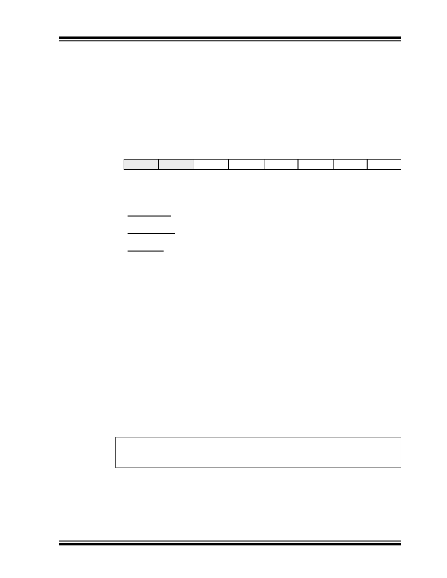
REGISTER 13-1:
CCP1CON REGISTER/CCP2CON REGISTER
U-0
R/W-0
—
DCxB1
DCxB0
CCPxM3
CCPxM2
CCPxM1
CCPxM0
bit 7
bit 0
bit 7-6
Unimplemented: Read as '0'
bit 5-4
DCxB1:DCxB0: PWM Duty Cycle bit1 and bit0
Capture mode:
Unused
Compare mode:
Unused
PWM mode:
These bits are the two LSbs (bit1 and bit0) of the 10-bit PWM duty cycle. The upper eight bits
(DCx9:DCx2) of the duty cycle are found in CCPRxL.
bit 3-0
CCPxM3:CCPxM0: CCPx Mode Select bits
0000
= Capture/Compare/PWM off (resets CCPx module)
0001
= Reserved
0010
= Compare mode, toggle output on match (CCPxIF bit is set)
0011
= Reserved
0100
= Capture mode, every falling edge
0101
= Capture mode, every rising edge
0110
= Capture mode, every 4th rising edge
0111
= Capture mode, every 16th rising edge
1000
= Compare mode,
Initialize CCP pin Low, on compare match force CCP pin High (CCPIF bit is set)
1001
= Compare mode,
Initialize CCP pin High, on compare match force CCP pin Low (CCPIF bit is set)
1010
= Compare mode,
Generate software interrupt on compare match (CCPIF bit is set, CCP pin is
unaffected)
1011
= Compare mode,
Trigger special event (CCPIF bit is set)
11xx
=PWM mode
Legend:
R = Readable bit
W = Writable bit
U = Unimplemented bit, read as ‘0’
- n = Value at POR reset
’1’ = Bit is set
’0’ = Bit is cleared
x = Bit is unknown
发布紧急采购,3分钟左右您将得到回复。
相关PDF资料
PIC16C54C-40/SS
IC MCU OTP 512X12 20SSOP
22-15-3033
CONN FFC/FPC 3POS .100 RT ANG
PIC18LC858T-I/PT
IC MCU OTP 16KX16 CAN 80TQFP
22-02-3033
CONN FFC/FPC VERTICAL 3POS .100
PIC18C858T-E/PT
IC MCU OTP 16KX16 CAN 80TQFP
PIC18C858T-I/PT
IC MCU OTP 16KX16 CAN 80TQFP
PIC18C658T-I/PT
IC MCU OTP 16KX16 CAN 64TQFP
PIC16LC717T-E/SS
IC MCU OTP 2KX14 A/D PWM 20SSOP
相关代理商/技术参数
PIC18C452T-E/PT
功能描述:8位微控制器 -MCU 32KB 1536 RAM 34I/O RoHS:否 制造商:Silicon Labs 核心:8051 处理器系列:C8051F39x 数据总线宽度:8 bit 最大时钟频率:50 MHz 程序存储器大小:16 KB 数据 RAM 大小:1 KB 片上 ADC:Yes 工作电源电压:1.8 V to 3.6 V 工作温度范围:- 40 C to + 105 C 封装 / 箱体:QFN-20 安装风格:SMD/SMT
PIC18C452T-I/L
功能描述:8位微控制器 -MCU 32KB 1536 RAM 34I/O RoHS:否 制造商:Silicon Labs 核心:8051 处理器系列:C8051F39x 数据总线宽度:8 bit 最大时钟频率:50 MHz 程序存储器大小:16 KB 数据 RAM 大小:1 KB 片上 ADC:Yes 工作电源电压:1.8 V to 3.6 V 工作温度范围:- 40 C to + 105 C 封装 / 箱体:QFN-20 安装风格:SMD/SMT
PIC18C452T-I/PT
功能描述:8位微控制器 -MCU 32KB 1536 RAM 34I/O RoHS:否 制造商:Silicon Labs 核心:8051 处理器系列:C8051F39x 数据总线宽度:8 bit 最大时钟频率:50 MHz 程序存储器大小:16 KB 数据 RAM 大小:1 KB 片上 ADC:Yes 工作电源电压:1.8 V to 3.6 V 工作温度范围:- 40 C to + 105 C 封装 / 箱体:QFN-20 安装风格:SMD/SMT
PIC18C601-I/L
功能描述:8位微控制器 -MCU 256KB 1536 RAM 26I/O RoHS:否 制造商:Silicon Labs 核心:8051 处理器系列:C8051F39x 数据总线宽度:8 bit 最大时钟频率:50 MHz 程序存储器大小:16 KB 数据 RAM 大小:1 KB 片上 ADC:Yes 工作电源电压:1.8 V to 3.6 V 工作温度范围:- 40 C to + 105 C 封装 / 箱体:QFN-20 安装风格:SMD/SMT
PIC18C601-I/L021
制造商:Microchip Technology Inc 功能描述:
PIC18C601-I/PT
功能描述:8位微控制器 -MCU 256KB 1536 RAM 26I/O RoHS:否 制造商:Silicon Labs 核心:8051 处理器系列:C8051F39x 数据总线宽度:8 bit 最大时钟频率:50 MHz 程序存储器大小:16 KB 数据 RAM 大小:1 KB 片上 ADC:Yes 工作电源电压:1.8 V to 3.6 V 工作温度范围:- 40 C to + 105 C 封装 / 箱体:QFN-20 安装风格:SMD/SMT
PIC18C601T-I/L
功能描述:8位微控制器 -MCU 256KB 1536 RAM 26I/O RoHS:否 制造商:Silicon Labs 核心:8051 处理器系列:C8051F39x 数据总线宽度:8 bit 最大时钟频率:50 MHz 程序存储器大小:16 KB 数据 RAM 大小:1 KB 片上 ADC:Yes 工作电源电压:1.8 V to 3.6 V 工作温度范围:- 40 C to + 105 C 封装 / 箱体:QFN-20 安装风格:SMD/SMT
PIC18C601T-I/PT
功能描述:8位微控制器 -MCU 256KB 1536 RAM 26I/O RoHS:否 制造商:Silicon Labs 核心:8051 处理器系列:C8051F39x 数据总线宽度:8 bit 最大时钟频率:50 MHz 程序存储器大小:16 KB 数据 RAM 大小:1 KB 片上 ADC:Yes 工作电源电压:1.8 V to 3.6 V 工作温度范围:- 40 C to + 105 C 封装 / 箱体:QFN-20 安装风格:SMD/SMT